A.-H. Chen, C.P. Dempsey, M. Pendharkar, A. Sharma, B. Zhang, S. Tan, L. Bellon, S.M. Frolov, C.J. Palmstrom, E. Bellet-Amalric, and M. Hocevar, Nanotechnology 35 075702
[Article] doi: 10.1088/1361-6528/ad079e
[Data set] doi: 10.5281/zenodo.7581136
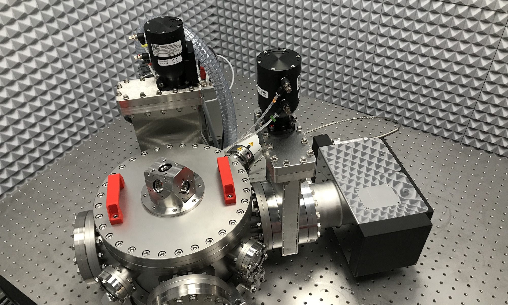
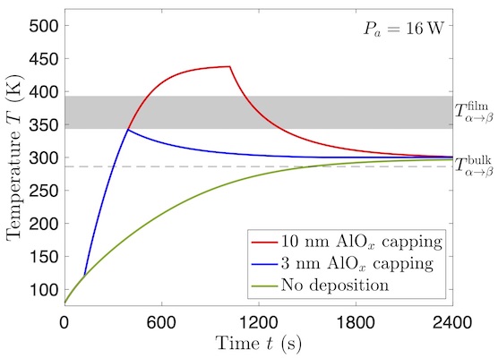
Metal deposition with cryogenic cooling is a common technique in the condensed matter community for producing ultra-thin epitaxial superconducting layers on semiconductors. However, a significant challenge arises when these films return to room temperature, as they tend to undergo dewetting. This issue can be mitigated by capping the films with an amorphous layer. In this study, we investigate the influence of different in situ fabricated caps on the structural characteristics of Sn thin films deposited at 80 K on InSb substrates. Regardless of the type of capping, we consistently observe that the films remain smooth upon returning to room temperature and exhibit epitaxy on InSb in the cubic Sn (α-Sn) phase. Notably, we identify a correlation between alumina capping using an electron beam evaporator and an increased presence of tetragonal Sn (β-Sn) grains. This suggests that heating from the alumina source may induce a partial phase transition in the Sn layer. The existence of the β-Sn phase induces superconducting behavior of the films by percolation effect. This study highlights the potential for tailoring the structural properties of cryogenic Sn thin films through in situ capping. This development opens avenues for precise control in the production of superconducting Sn films, facilitating their integration into quantum computing platforms.